
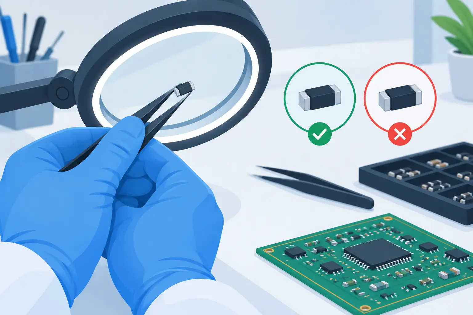
A single reversed SMD diode can turn a routine power-up into a fault-finding session. A backward polarized capacitor may survive just long enough to pass a basic test, then fail in service. Polarity errors are small placement mistakes with outsized consequences, which is why SMT component polarity checking belongs in both assembly verification and repair workflow.
The challenge is not simply identifying a plus or minus mark. Board silkscreen, package markings, CAD library conventions, reel orientation, and the actual circuit function must agree. When they do not, the schematic and manufacturer datasheet take priority over a hurried visual assumption.
What Requires SMT Component Polarity Checking?
Many common chip resistors, ceramic capacitors, and inductors are non-polarized. They can generally be placed in either direction unless orientation is needed for marking visibility, automated inspection, or process control. The parts that demand deliberate inspection are polarized or direction-sensitive devices.
Diodes are the most familiar example. Their anode and cathode orientation controls current flow, and a reversed rectifier, TVS diode, Schottky diode, or signal diode can prevent a circuit from operating correctly. LEDs are also diodes, but their polarity can be less obvious once the package is installed. Electrolytic, tantalum, and polymer capacitors require correct positive and negative terminal placement. Incorrect orientation can create leakage, overheating, or catastrophic failure depending on the capacitor type and applied voltage.
Integrated circuits are orientation-sensitive even when the term polarity is not technically precise. Pin 1 must match the PCB land pattern. Transistors, MOSFETs, bridge rectifiers, optocouplers, battery holders, and many connectors also have a fixed orientation that must be verified before power is applied.
Read the Part Before Reading the Board
Reliable checking starts with the component datasheet. Package marks are not universal across manufacturers, and visual conventions vary by package family.
For a typical SMD diode, a band identifies the cathode. The PCB footprint commonly uses a bar at the cathode end, but artwork can be incomplete, covered by solder, or visually ambiguous on a dense board. Match the physical band to the footprint bar, then confirm that location against the schematic reference designator and diode symbol.
LED markings vary more than many technicians expect. A chamfered corner, a green mark, a notch, a shortened pad, or a feature in the internal lead frame may indicate cathode or anode depending on the package. Never apply a general LED rule to an unfamiliar package. Check its datasheet drawing, especially for side-view and bottom-view conventions.
Polarized capacitor markings also need careful interpretation. Most tantalum and polymer SMD capacitors mark the positive terminal with a stripe or plus sign. Aluminum electrolytic chip capacitors often mark the negative side. That difference is enough to create errors when an operator relies on appearance rather than the part documentation. The PCB itself may use a plus symbol, a shaded half-circle, or a distinctive pad shape, but these are design choices rather than universal standards.
For ICs, use the pin-1 dot, molded dimple, bevel, or corner mark specified for that exact package. A large orientation mark on the top of a QFN, BGA, or DFN may not be visible after placement. Assembly documentation should include a clear pin-1 reference image before boards reach the line.
Use a Layered Verification Process
The most dependable process checks polarity at more than one stage. Catching an issue before reflow is faster than diagnosing it after a board has been powered, but post-assembly verification remains valuable when a board has been reworked or its history is unknown.
At incoming inspection, compare the manufacturer label, internal part number, and reel orientation against the approved bill of materials and placement data. A correct-looking component on the wrong reel is still a production error. For parts with subtle marks, retain a magnified reference image in the work instruction.
Before placement, verify that the PCB footprint matches the schematic symbol and the datasheet-recommended land pattern. This is where library errors are found. A board can be assembled exactly as programmed and still be wrong if an anode, cathode, or pin-1 convention was reversed in the footprint. First-article inspection should confirm a sample of every polarity-sensitive reference designator, not only the first diode or capacitor encountered.
After reflow, inspect under adequate magnification and lighting. Look for the physical cathode band, capacitor stripe, LED package feature, or IC pin-1 mark relative to the board indicator. Automated optical inspection is useful for high-volume work, particularly where known package features are clear and repeatable. It is not a substitute for validated component libraries or an inspector who understands the component’s actual marking.
For repair work, begin with photographs if the device arrived intact. A close image can preserve the original orientation before hot air, flux residue, or lifted pads obscure the evidence. If the original part is missing, use the schematic, board layout, nearby channels, and the component datasheet to establish orientation. Do not copy an adjacent board blindly if its revision or population options are unknown.
Confirm Orientation Electrically When Visual Marks Are Unclear
Electrical checks provide a valuable second opinion, especially on suspect repairs and densely populated boards. They must be interpreted in circuit context.
A diode-test function can often identify a diode’s forward direction. With the positive probe on the anode and the negative probe on the cathode, a standard silicon diode usually shows a forward voltage drop. Reversing the probes should show an open or much higher reading. A low-drop Schottky diode and an LED will produce different values, but the directional behavior remains useful. Parallel components, protection networks, and semiconductor junctions can create misleading in-circuit readings, so isolate one terminal when the result is ambiguous.
For LEDs, a controlled LED test function can verify both direction and illumination. Use a test current appropriate for the device and avoid assuming that a meter’s diode mode will safely light every LED string. High-brightness, blue, white, and series-connected LEDs may require more voltage than a basic diode test supplies.
Capacitor polarity cannot normally be proven by a quick capacitance reading alone. A reversed polarized capacitor may still show a plausible capacitance value at low test voltage. Confirm the marked terminal against the schematic rail and footprint marking, then inspect for leakage, elevated ESR, or heat if the board has been energized. Power should be removed and capacitors discharged before measurement.
Handheld tweezer-style instruments are particularly useful for checking nearby passive values, ESR, and component identity during SMT troubleshooting. They help establish whether a fitted part matches its expected resistance, capacitance, or inductance, but measurement does not replace visual confirmation of a polarized part’s direction. The two methods answer different questions: one checks value and condition, while the other checks orientation.
Common Failure Points in Production and Repair
Polarity mistakes often originate upstream of placement. A mirrored footprint, a copied library symbol, an unrevised assembly drawing, or an undocumented substitute component can defeat an otherwise careful process. The risk rises when packages are tiny, labels are abbreviated, and multiple vendors supply electrically similar parts with different marking conventions.
Rework introduces a separate set of risks. Heat can fade package marks. Flux can hide a PCB bar or plus symbol. A technician focused on removing a damaged component may lose the original orientation reference. Document the location before removal, clean the pads before replacement, and compare the replacement package to its datasheet rather than to memory.
There is also a trade-off between speed and certainty. On a high-volume line, machine-readable placement data and optical inspection improve throughput. On prototypes, low-volume repair, and mixed boards, a short manual check against the schematic is often the fastest way to prevent a costly repeat cycle. The right balance depends on volume, package density, and the consequence of failure.
Build Polarity Checks Into the Work Instruction
A useful work instruction does more than say “verify polarity.” It identifies the exact board reference, shows the correct package orientation, names the component mark to inspect, and points to the authoritative datasheet when needed. For critical parts, include both a pre-reflow and post-reflow signoff point.
Keep the instruction practical. Call out high-risk items such as reverse-polarity protection diodes, polarized capacitors on power rails, status LEDs, battery connections, and pin-1-sensitive ICs. If a design has repeated channels, verify every channel rather than assuming the first correct placement proves the rest.
Good SMT component polarity checking is a disciplined comparison of documentation, physical markings, board artwork, and electrical behavior. Treat it as a repeatable inspection step, not a last-minute visual glance, and polarity errors become far easier to prevent than to troubleshoot.